
![]()
PSpice 9.2 Simulation Tutorial By Joey Hernandez TCI #86508
Home | Resistor Color Code| Capacitor Codes | OP Amps | 555 Timer | Logic Gates
Pspice Tutorials |Projects | Electronic Component Data Sheets | Links | Programs |
This is a simulation of basic Voltage Divider Circuit involving two resistors and one power source. The tutorial has been prepared assuming that it is the first time using PSpice. Other simulations in this web site will contain less detail because once you simulate two or three circuits the procedures will appear routine and you will move through them quickly. After some practice you will discover that there is more than one way to do certain procedures. I have tried to be as detailed as possible to benefit beginners. Personally I learned through different sources including a Basic Computing class at Technical Career Institute, New York City, however, the true teacher is the hands on trial and error method. I certainly hope these tutorials are helpful. Enjoy.
Sincerely,
Joey Hernandez
If Orcad PSpice 9.2 Lite Edition is not installed in your computer you can download it from Orcad's website http://www.orcad.com/downloads/demo/default.asp or you can request Orcad to send you the free cd. You will find that the free version of PSpice is surprisingly vast in its capabilities and it does not expire.
Lets Begin
1. Open Orcad PSpice 9.2 Lite Edition.
<START>
<PROGRAMS>
<ORCAD 9.2 FAMILY RELEASE 9.2 LITE EDITION>
<CAPTURE LITE EDITION>
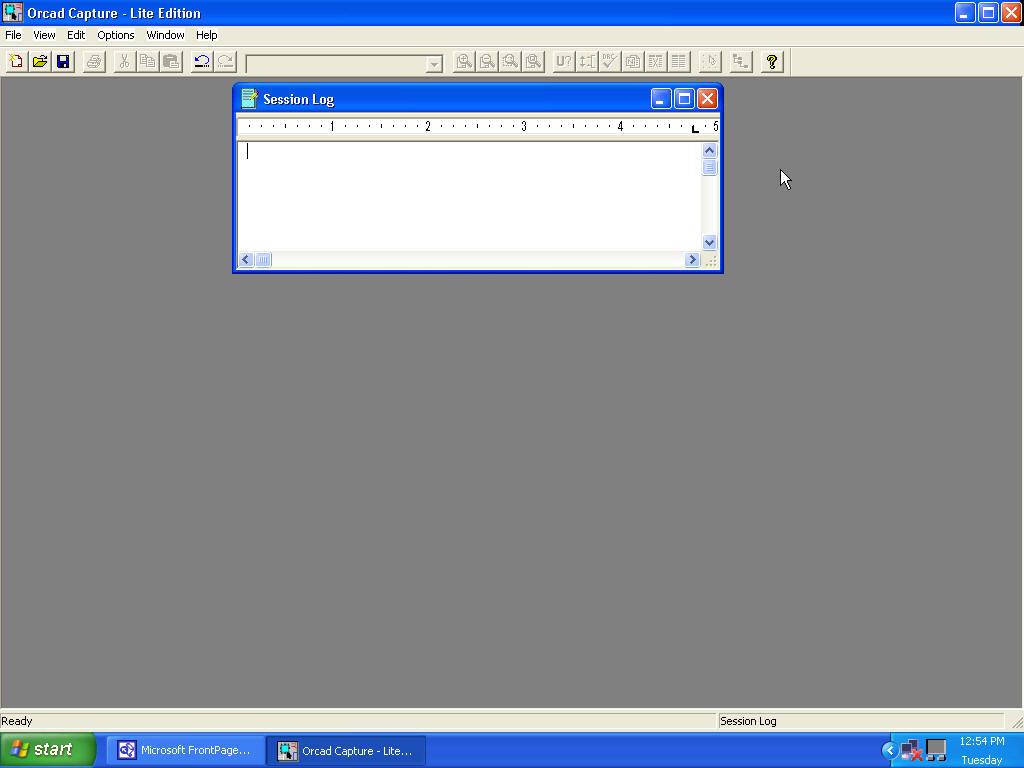
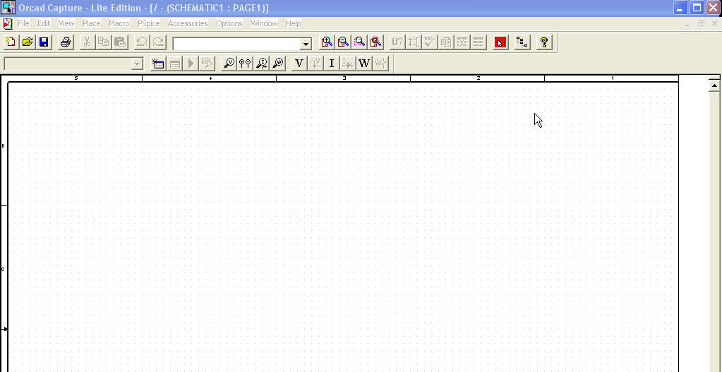
2. Once the program is opened you will see the following screen.
This is like the desktop of the program that holds different screens of the program.
3.
On the top of the page you will see menus.
To start a new project follow the following steps. Go to the top of the screen to the toolbar and
use the sequence <FILE> <NEW> <PROJECT>.
The following New Project dialog box will appear:
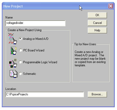
Assign your project a name, select Analog or Mixed A/D, and enter a location where you want
the project to be saved. Press OK.
4. The following Create PSpice Project dialog box will appear.
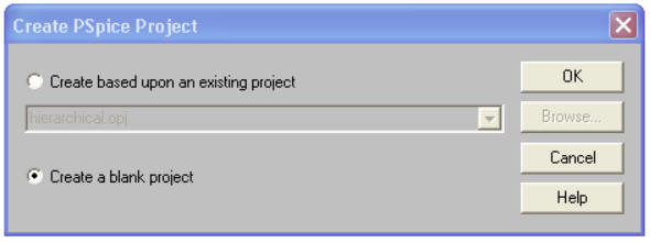
Select the Create blank project radio button and press OK.
5. The following windows will appear.
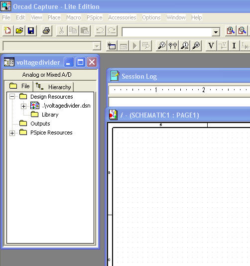
Maximize the SCHEMATIC 1 : PAGE 1 screen.
The screen should now look like the following picture:
6. Now it is time to build the circuit.
If this is the first time that PSpice is being used, the component libraries have to be added.
Go to the top of the screen to the toolbar and use the sequence <PLACE> <PART>.
The following Place Part dialog box will appear:

Click Add Library
The following Browse File box will appear:

Select (source) and click Open.
Now the source library will appear in the place part dialog box as shown in the following
picture:
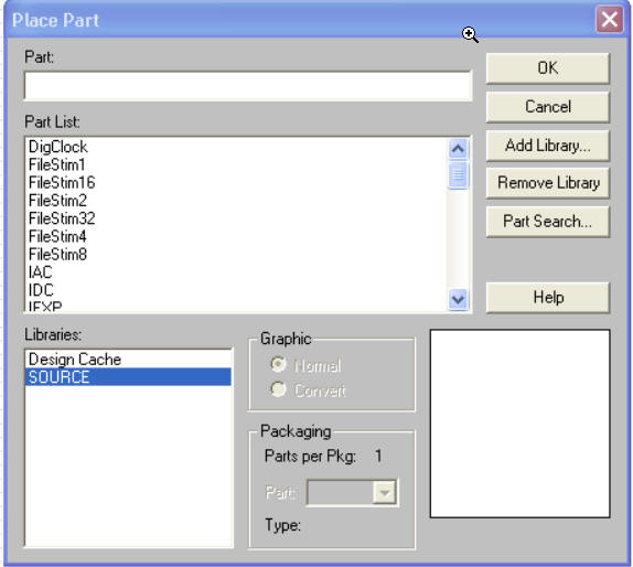
Click Add Library and add two more libraries (eval) and (analog).
Now The Place Part dialog box will have the libraries needed to construct the voltage divider
circuit.
7. To place the first parts for this simulation ( a resistor ), highlight the ANALOG library by left
clicking on it. Next either type the letter R in the Part text box or scroll through the Parts
list until you find the letter R and highlight it by left clicking on it once.
The Place Part box should look as follows:
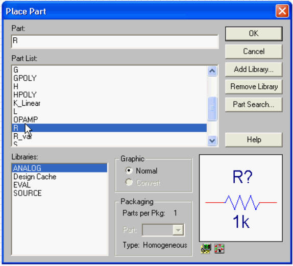
Notice that a graphical representation of the part is shown on the lower right hand corner of
the Place Part box.
Once you have selected the part click OK.
8. Now the part selected is controlled by the position of the mouse pointer.
Place the part in the desired position on the Schematic page and left click once.
The following picture shows the resistor being placed on the schematic page:
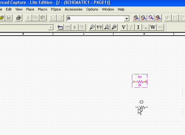
Notice that the resistor is automatically named R1 and it is highlighted.
After the part is placed the mouse pointer will continue to hold the same part type allowing for
multiple placements of parts.
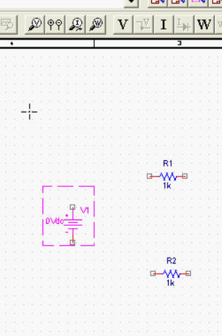
9. Place the second resistor in the desired position and left click once.
To exit this mode right click and from the drop down menu select End Mode.
The following picture shows the procedure:
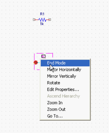
Notice that the drop down menu has choices so that you can rotate the part or mirror it horizontally
or vertically. When you rotate the part it will rotate 90 degrees. Zoom in and out is useful when you
are wiring the parts together. Edit properties can be used to alter the parts behavior. You will
probably not have to use this feature however if needed you can alter the part and it will not be
affected for other simulations. Go to will place the crosshatch to a point in the screen that that you
can select from the Go to dialog box.
10. To place the voltage source for this simulation go to the top of the screen to the toolbar and
use the sequence <PLACE> <PART>.
Highlight the SOURCE library by left clicking on it. Next either type VDC in the Part text box
or scroll through the Parts list until you find VDC and highlight it .
The Place Part box should look as follows:
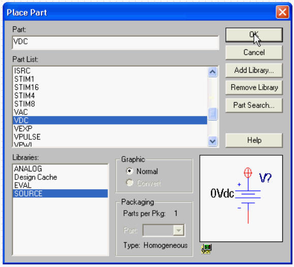
Notice that a graphical representation of the part is shown on the lower right hand corner of
the Place Part box. Once you have selected the part click OK.
11. Now the part selected is controlled by the position of the mouse pointer.
Place the part in the desired position on the Schematic page and left click once.
The following picture shows the voltage source being placed on the schematic page:
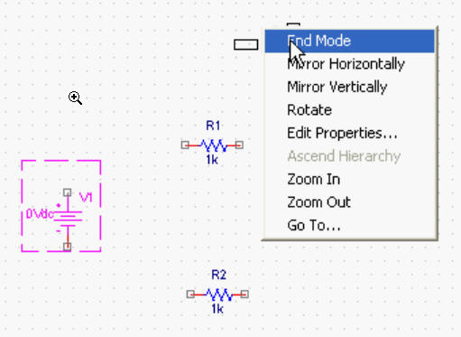
Notice that the voltage source is automatically named V1 and it is highlighted.
After the part is placed the mouse pointer will continue to hold the same part type allowing for
multiple placements of parts.
. To exit this mode right click and from the drop down menu select End Mode.
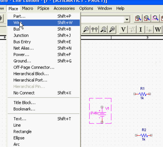
12. Now that the parts needed to construct the circuit are in place, they have to be connected to
one another. Go to the top of the screen to the toolbar and use the sequence <PLACE> <WIRE>.
The following picture shows the procedure:
The mouse pointer will turn into a crosshatch as shown in the following picture:
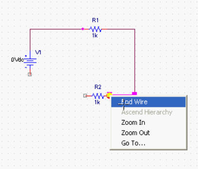
13. Move the crosshatch to one end a component and once in position left click once and proceed to
the end of the next component you want to connect to. Once you are in place double click and
then right click and select End Wire from the drop down menu.
The following picture shows the procedure:
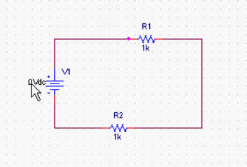
14. After the parts have been connected together you can rename the parts and change their value by
double clicking on the labels. V1 in this circuit will be changed to 10V.
Double click on V1's value (0V) as shown in the following picture:
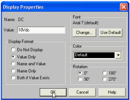
A Display properties dialog box will appear.
Change the value to 10Vdc as shown in the following picture:
15 .The circuit will not produce a simulation if it is not grounded.
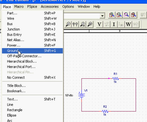
To place a ground go to the top of the screen to the toolbar and use the sequence <PLACE>
<GROUND> as shown in the following picture:
The following Place Ground dialog box will appear:
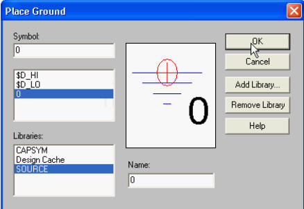
Highlight (SOURCE) in libraries and highlight (0). Click OK.
Place the ground in the desired position and wire it to the circuit following the same procedure used to
wire other parts ( step 9 ).
The circuit is now complete .
16. To simulate the circuit a simulation profile must be established.
To accomplish this go to the top of the screen to the toolbar and use the sequence <PSPICE>
<NEW SIMULATION PROFILE >.
The following picture shows the procedure:

A New Simulation dialog box will appear as shown in the following picture.
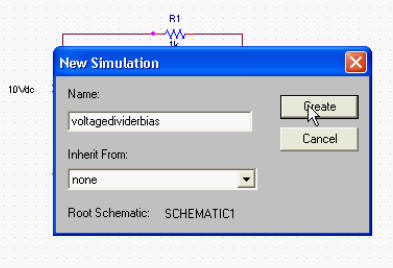
Name the simulation and click Create.
A Simulation Settings window will appear as shown in the following picture:
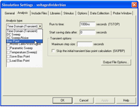
For this simulation select Bias Point as the analysis type and click OK
The window will be modified and will appear as follows:
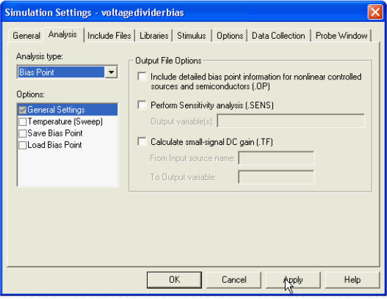
Click Apply then OK.
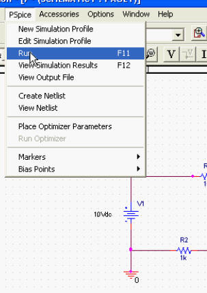
17. Now its time to run the simulation.
Go to the top of the screen to the toolbar and use the sequence < PSPICE > < RUN >.
The following picture shows the procedure:
After a few seconds the following window will appear:
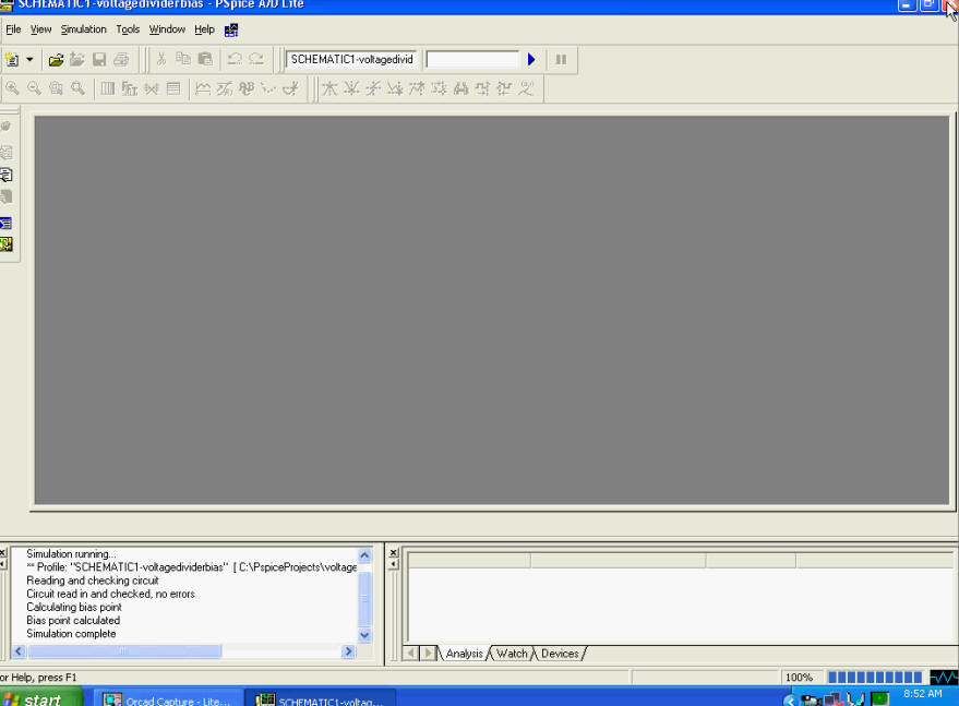
Close this window.
Now the schematic page will appear with the circuit as shown in the following picture:
Click on (V) to see voltages, (I) to see currents and (W) to see power.
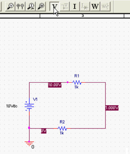
Click on (V) to see voltages, (I) to see currents and (W) to see power.
The circuit is now simulated and the results are shown in the following picture:
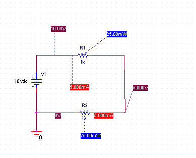
The voltage, current and power displays can be moved with the mouse to any desired position and they can be deleted as well.
You can copy and past the circuit into a word processor document such as Microsoft Word by left clicking the mouse and holding the left click button down while you move over a selected area. Once selected the area selected will turn pink. Go to the top of the screen to the toolbar and use the sequence <EDIT> <COPY> then past to your document.This will prove to be very helpful if you are writing laboratory reports for school.
18. To close the project go to the top of the screen to the toolbar and use the sequence <FILE> <CLOSE>
The following window will appear:
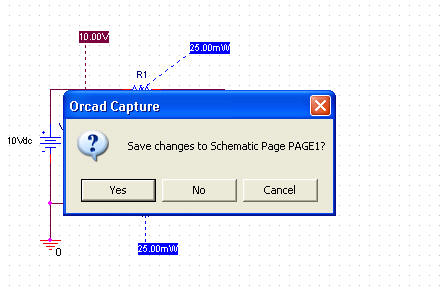
Click Yes.
The following window will appear:
You can start a new project or you can exit the program by going to the top of the screen to the toolbar
and use the sequence <FILE> <EXIT>.
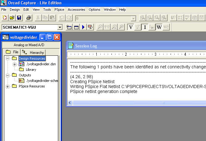
***Pspice project files are voluminous,
therefore, a floppy disk might not
have sufficient space to save the
files. Orcad Pspice will automatically
select its default location-
C:\PspiceProjects.***